


| Equipment model | AVI-IC-A025C |
|---|---|
| CCDAnalysis accuracy(μm/pixel) | 2.5( front side )、5(back side)(16K High color accuracy CCD) |
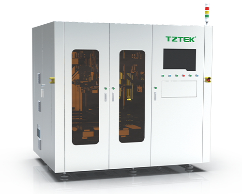
| Dimensions(mm) | 1790×2250×1990(L×W×H) |
| Equipment weight(t) | 3 |
| Equipment power(Vac,Hz,KW) | 380,50,16 |
| Processing method | Fully automatic double-sided scanning, NG tank, waiting tank |
| camera type | Black and white / color linear camera |
| Detection area(mm) | 30×50(MIN) 120×260(MAX) |
| CT(pnl/h) | Board width<40 mm(scan once):270 40 mm≤Board width<80 mm(Scan twice):200 80 mm≤Board width<120 mm(Scan three times):140 (Double-sided inspection) |
| Reference format | Gerber (RS274X)、ODB++ |
| Detecting plate thickness(mm) | 0.06-2 |
| Defect confirmation | VRS Offline judgment |
| Defect scope | Copper surface area covered by gold surface/organic soldering flux: scratches, pinholes, gold particles, metal bumps, dents, discoloration, copper leakage, contamination, chips, insufficient etching, over-etching, foreign matter, no gold plating Solder protection area: scratches, exposed copper, foreign matter, ink peeling, ink offset, contamination, ink cracks, short circuit under the ink, etc. |
| Applicable version range | Substrate Type:PBGA、CSP、 RF、 COB、 OSP、BOC、MMG、WBGA、PSAP、MCM-BGA、FCBGA、uBGATM |
| Testing materials | Can be used for FR4, FR5, aluminum substrate, reverse copper foil, etc. |
| Temperature and humidity | 22±2℃,50±10% |